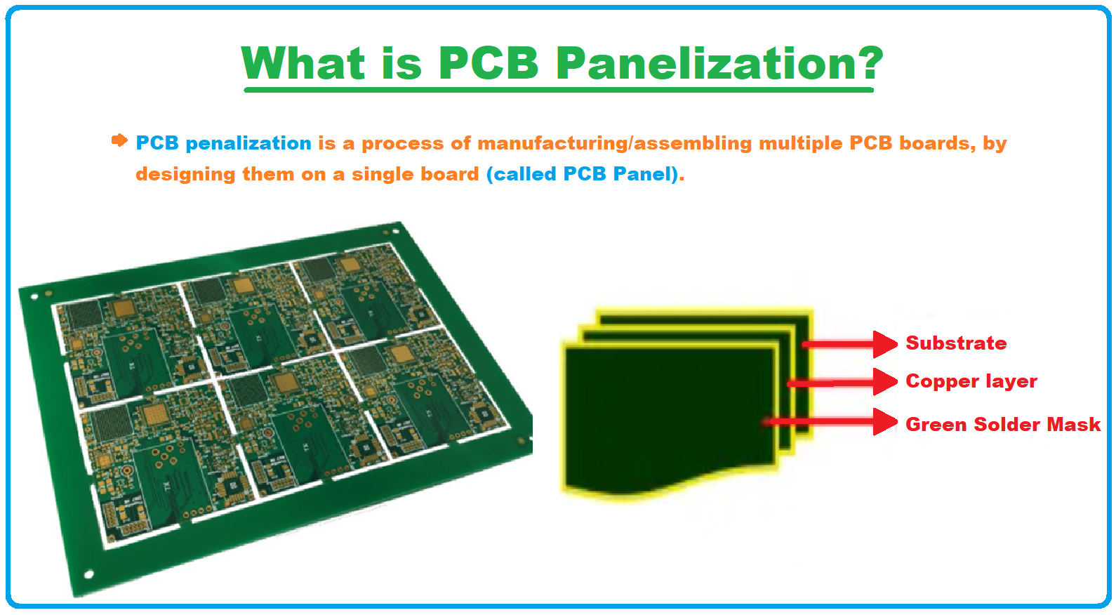
Panelization
PCB panelization is a manufacturing technique in which smaller boards are manufactured en-masse connected together as a single array, making it easier
to move through an assembly line. The individual boards can easily be depanelized or removed from the array for packaging or installation into a product.
Alternatively a PCB processing edge around an individual board to increase its width to fit on the assembly line.
In order to reap the benefits of mass production that come with panelization,
it’s important to factor in the following design considerations:
- 1) PCB-array strength. There’s a tradeoff between the ease of depanelization and array integrity during production.
Increasing board count per array can increase strength and reduce vibration.
- 2) Component layout. Placement of components and connectors, especially those hanging off the edge of a
board can limit your panelization options. Be mindful of the location of sensitive SMT (surface mount technology)
components towards the edge of a board.
- 3) PCB shape. The shape of your board can complicate panelization. Rectangles are ideal, but if the shape of your board is
complex, alternating images from 90° to 180° can help you maximize space on a panel. Use a CAD program to fit unusually shaped
boards into an array.
- 4) Tooling holes. Arrays and break-away processing edges can give you space for tooling holes for automated testing on the assembly line.
Advantages of PCB Panelization
PCB panelization doesn’t just help smaller boards fit in standard production processes,
it also makes production more efficient. Common advantages of PCB panelization include:
- • Mass production. If you need to build a lot of boards, panelization will save you time and money.
- • Product safety. Panelization protects the PCB from shock and vibration experienced during assembly.
- • Speed and efficiency. From paste printing to component assembly, soldering, and even testing—it’s faster
and more efficient to process multiple boards at once as part of a large array.
- • Standard panel sizes. It’s often more cost effective to manufacture boards using the fabricator’s
standard processing panel.
Every manufacturer has their own preferences for panel sizes, but in general 18 x 24 inch panels with ½ inch perimeter of clearance for handling double-sided boards (1 inch for multilayer boards) are standard. You’ll want to check with your fabricator before drafting a panel for their assembly process.